PDF version: Notes on Digital Electronics – Logan Thrasher Collins
Logic gates
In digital electronics, circuit components (e.g. transistors, resistors, etc.) can be organized to form logic gates. Logic gates take input signals and determine output signals according to simple rules. Different logic gates exhibit distinct rules. Fundamental logic gates in digital electronics include the NOT gate (also called an inverter), AND gate, OR gate, NAND gate, NOR gate, XOR gate, and XNOR gate. The rules for these gates are given in the following table.
It should be noted that there are also versions of these logic gates which take more than two inputs. For example, an AND gate with three inputs would require a signal value of 1 for all three inputs in order to give an output of 1.
NAND gates and NOR gates have alternative symbols (relative to the ones in the previous table) in certain situations. The following two paragraphs describe the reasons for these alternative symbols.
When a NAND gate is used to take one or more 0 inputs (i.e. 00, 01, 10 for a device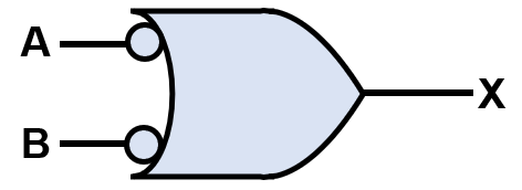 with two inputs), it acts as a “negative-OR” gate. In this case, any of the 0 inputs will give an output of 1, so the operation is similar to OR. The symbol for a negative-OR version of a NAND gate is given at right.
When a NOR gate is used to take all 0 inputs (i.e. 00 for a device with two inputs), it acts  as a “negative-AND” gate. In this case, all the 0 inputs together will give an output of 1, so the operation is similar to AND. The symbol for a negative-AND version of a NOR gate is given above.
Boolean algebra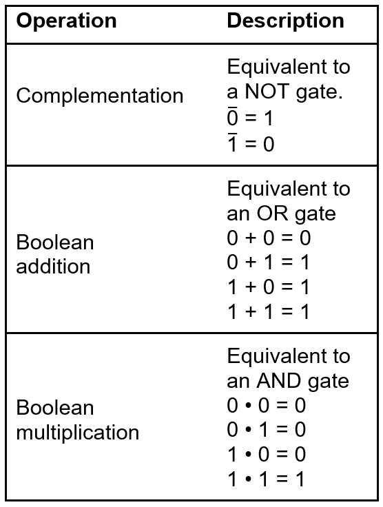
Boolean algebra provides a mathematical way of representing the behaviors of logic gates. Complementation, Boolean addition, and Boolean multiplication are important operations in Boolean algebra. These are shown in the table to the right. Combining these operations allows complex logic gate arrangements to be described. Note that any variable or its complement is referred to as a “literal” in the language of digital logic.
The distributive law, the commutative addition and multiplication laws, and the associative addition and multiplication laws are the same in Boolean algebra as in ordinary algebra. As a result, logic gate arrangements are subject to these laws.
There are twelve basic rules for Boolean algebra which are often useful for analyzing logic gates. They are listed in the box below.

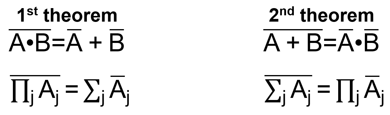
DeMorgan’s theorems are useful tools for simplifying Boolean expressions. DeMorgan’s first theorem states that the complement of a Boolean product of variables equals the sum of the complements of the variables. DeMorgan’s second theorem states that the complement of a Boolean sum of variables equals the Boolean product of the complements of the variables. DeMorgan’s theorems also extend to expressions with more than two variables. DeMorgan’s first and second theorem are given below in the form with two variables and the form with n variables.
SOP and POS forms
There are two forms into which Boolean expressions can be converted via simple algebraic methods; the sum-of-products (SOP) form and the product-of-sums (POS) form. These forms make it easier to use Boolean expressions for digital electronics. To understand these forms, note that the domain of a Boolean expression is the set of variables (either complemented or uncomplemented) which appear in the expression.
The SOP form is exactly as its name suggests, a sum of terms which consist of products of literals (e.g. AB̅ + AC). The SOP form can also include terms which consist of a single literal. To implement the SOP form using logic gates, the following methods can be used. The first is to connect the output terminals of two or more AND gates to the input terminals of an OR gate. The second is to connect the output terminals of one or more NAND gates to the input terminals of another NAND gate (which operates in the negative-OR mode).
There is also a standard SOP form which is distinct from the regular SOP form. The standard SOP form is one in which all of the variables in the domain appear in each term of the expression. To convert a SOP expression into its standard form, multiply each nonstandard term by a sum of the missing variable and the missing variable’s complement. Repeat this until all of the terms contain all the variables in the domain either in complemented or uncomplemented form. As an example, consider the domain {A, B, C} and the SOP expression AB̅ + AC. Perform the operation AB̅(C + C̅) + AC(B + B̅) = AB̅C + AB̅C̅ + ABC. Now the expression is in standard SOP form (note that one of the AB̅C terms vanished as a result of the basic rules of Boolean algebra).
When looking at the binary representation of a standard SOP term, only a single combination of variable values will make the term equal to 1. Furthermore, a standard SOP expression will only equal 1 if at least one of its terms are equal to 1.
The POS form is also exactly as its name suggests, a product of terms which consist of sums of literals. An example of this is (A̅ + B)(A + B̅ + C). The POS form can also include terms which consist of a single literal. However, a complementation overbar cannot extend to more than one term in a POS expression. To implement the POS form using logic gates, the following methods can be used. The first is to connect the output terminals of two or more OR gates to the input terminals of an AND gate. The second is to connect the output terminals of one or more NOR gates to the input terminals of another NOR gate (which operates in the negative-AND mode).
There is a standard POS form which is distinct from the regular POS form. The standard POS form is one in which all of the variables in the domain appear in each parentheses-enclosed sum term of the expression. To convert a POS expression into its standard form, add a product of the missing variable and its complement (e.g. AA̅) inside each parentheses-enclosed sum term. Next, apply the basic Boolean algebra rule that A + BC = (A + B)(A + C). Repeat this until the POS expression is in standard form. As an example, consider the domain {A, B, C} and the POS expression (A̅ + B)(A + B̅ + C). Perform the operation (A̅ + B + CC̅)(A + B̅ + C) = (A̅ + B + C)(A̅ + B + C̅)(A + B̅ + C). Now the expression is in standard POS form.
When looking at the binary representation of a standard POS sum term (parentheses-enclosed term), only a single combination of variable values will make the term equal to 0. Furthermore, a standard POS expression will only equal 0 if at least one of its parentheses-enclosed sum terms are equal to 0.
Truth tables
When working with Boolean expressions and digital electronics, a truth table provides a valuable way of representing the logical operation of a circuit. Furthermore, standard SOP and POS expressions can be determined using truth tables. A truth table is a listing of the possible combinations of input variable values and corresponding output values for a given Boolean expression.
To convert a standard SOP or POS expression into truth table format, first list all of the possible combinations of binary values (2n possibilities where n is the number of variables). Next, places 1s in the output column for all of the binary values that make the standard SOP or POS expression equal to 1 and place 0s in the output column for all of the binary values that make the standard SOP or POS expression equal to 0. Recall that a standard SOP expression will equal 1 if at least one of its terms are equal to 1 and that a standard POS expression will equal 0 if at least one of its parentheses-enclosed sum terms are equal to 0. The following tables are examples of truth tables for a SOP expression (left) and a POS expression (right).

To determine the standard SOP expression represented by a truth table, list the binary values for which the output is 1. Convert each binary value of 1 into its corresponding variable and each binary value of 0 into its corresponding complemented variable. This will produce the terms of the SOP expression which are then added together.
To determine the standard POS expression represented by a truth table, list the binary values for which the output is 0. Convert each binary value of 0 into its corresponding variable and each binary value of 1 into its corresponding complemented variable. This will produce the parentheses-enclosed sum terms of the POS expression which are then multiplied together.
Organization of Karnaugh maps
The Karnaugh map gives a systematic method for simplifying Boolean expressions. It can produce the simplest possible SOP or POS expression for a given problem. Karnaugh maps can be employed for expressions of two, three, four, or five variables. Note that there are also other algorithms, the Quine McCluskey method and the Espresso algorithm, which work on expressions with five or more variables. These more advanced algorithms are more readily automated by software as well. Nonetheless, Karnaugh maps represent a useful exercise for thinking about digital logic design.
The three-variable Karnaugh map is an array of eight cells (as shown below at left) with the possible binary values for A and B given along the rows and the possible binary values for C given along the columns. The four-variable Karnaugh map is an array of sixteen cells (as shown below at right) with the possible binary values for A and B given along the rows and the possible binary values for C and D given along the columns.

Karnaugh maps are arranged such that there is only a single change between any two adjacent cells. Two cells are physically adjacent if they are touching via the top, bottom, left side, or right side (diagonals do not count). Adjacency also extends to the cells at opposite edges of the tables. That is, the tables “wrap around” so that cells at the top are adjacent to corresponding cells at the bottom and cells at the left side are adjacent to corresponding cells at the right side.
Karnaugh maps with SOP and POS expressions
To map a standard SOP expression, place a 1 on the Karnaugh map for each term that is part of the expression. Make sure to place the 1s on the cells which match that term of the expression (e.g. A̅BC̅ goes in the 010 cell of a three-variable Karnaugh map). To map a nonstandard SOP expression, it must first be converted to standard SOP expression. This conversion is often carried out using a binary-based version of the method outlined earlier.
Karnaugh maps are often used to construct minimized SOP expressions (after starting with standard SOP expressions). By contrast to standard SOP expressions, minimized SOP expressions contain the fewest possible terms and the fewest possible variables per term. Minimized SOP expressions are usually implementable with fewer logic gates than standard SOP expressions.
To minimize a standard SOP expression, first perform the process of grouping the 1s. The goal of grouping the 1s is to maximize the size of the groups and minimize the number of groups. For Karnaugh maps of three or four variables, any individual group must consist of 1, 2, 4, 8, or 16 cells. Each cell in a group must be adjacent to one or more cells in the  same group (but not all cells in a group need to be adjacent). Each group must contain the largest possible number of 1s. Finally, each 1 on the map must be included in at least one group. Note that a 1 can be included in overlapping groups so long as each of the groups involved also have noncommon 1s. At right, an example of grouping the 1s is displayed.
The next step in minimizing a standard SOP expression is to analyze the groups of 1s. Each group of cells with 1s creates a product term composed of all of the variables in that group which occur in only the complemented or only the uncomplemented form. Any variables which occur in both forms within the group are eliminated. The remaining variables in a given group comprise a term within the minimized SOP expression. All of the terms from the groups are summed to find the full minimized SOP expression.
To use Karnaugh maps with truth tables for standard SOP expressions, place the 1s on the map according to the binary input values and the binary output values described by the truth table (e.g. if the truth table has a value of 101 for the SOP expression AB̅C, put a 1 on the corresponding 101 cell of the Karnaugh map).
Certain binary values are not used in certain applications. For instance, when encoding integers through binary, there are sixteen possible combinations of binary digits but only the integers 0 through 9 need to be represented (ten values). The other six combinations of binary digits are invalid. Since these binary values will never actually occur, their outputs can be treated as either 0 or 1. On Karnaugh maps, these are called “don’t care” terms. “Don’t care” terms are placed on the Karnaugh map as an X and treated as 1 if they help to make a larger group. If a “don’t care” term does not help to make a larger group, it is treated as a 0 output. By helping to make larger groups of 1s, “don’t care” terms can aid in further simplifying SOP expressions and allowing less logic gates to be used.
To map a standard POS expression, place a 0 on the Karnaugh map for each parentheses-enclosed sum term that is part of the expression. Make sure to place the 0s on the cells which match that term of the expression (e.g. (A̅ + B + C̅) goes in the 101 cell of a three-variable Karnaugh map). To map a nonstandard POS expression, it must first be converted to standard POS expression. This conversion is often carried out using a binary-based version of the method outlined earlier.
Karnaugh maps are often used to construct minimized POS expressions (after starting with standard POS expressions). By contrast to standard POS expressions, minimized POS expressions contain the fewest possible terms and the fewest possible variables per term. Minimized POS expressions are usually implementable with fewer logic gates than standard POS expressions.
To minimize a standard POS expression, first perform the process of grouping the 0s. The rules for doing so are identical to the rules for grouping the 1s as outlined in the previous section, except that 0s are used. The next step in minimizing a standard POS expression is to analyze the groups of 0s. This is also carried out in the same way as that described for the SOP version of the process. After doing this, the remaining variables in a given 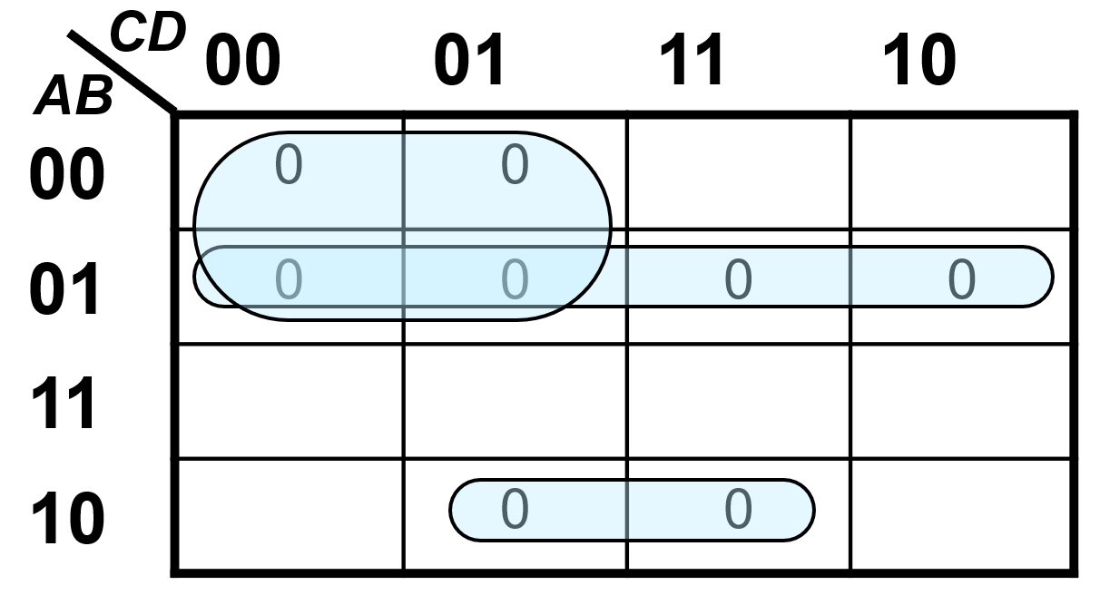 group comprise a parentheses-enclosed sum term within the minimized POS expression. All of the parentheses-enclosed sum terms from the groups are multiplied to find the full minimized POS expression. “Don’t care” terms are also applied the same way for standard POS expressions as they are for standard SOP expressions.
To use Karnaugh maps with truth tables for standard POS expressions, place the 0s on the map according to the binary input values and the binary output values described by the truth table (e.g. if the truth table has a value of 101 for the POS expression AB̅C, put a 0 on the corresponding 101 cell of the Karnaugh map).
Karnaugh maps can be used to convert between standard SOP and standard POS expressions. This is useful to help compare the minimized versions of the expressions and to see if one of the two can be implemented using fewer logic gates than the other. For going from SOP to POS, all of the cells which do not contain 1s must instead contain 0s. These 0 cells encode the equivalent POS expression. For going from POS to SOP, all of the cells which do not contain 0s must instead contain 1s. These 1 cells encode the equivalent SOP expression.
Basic combinational logic
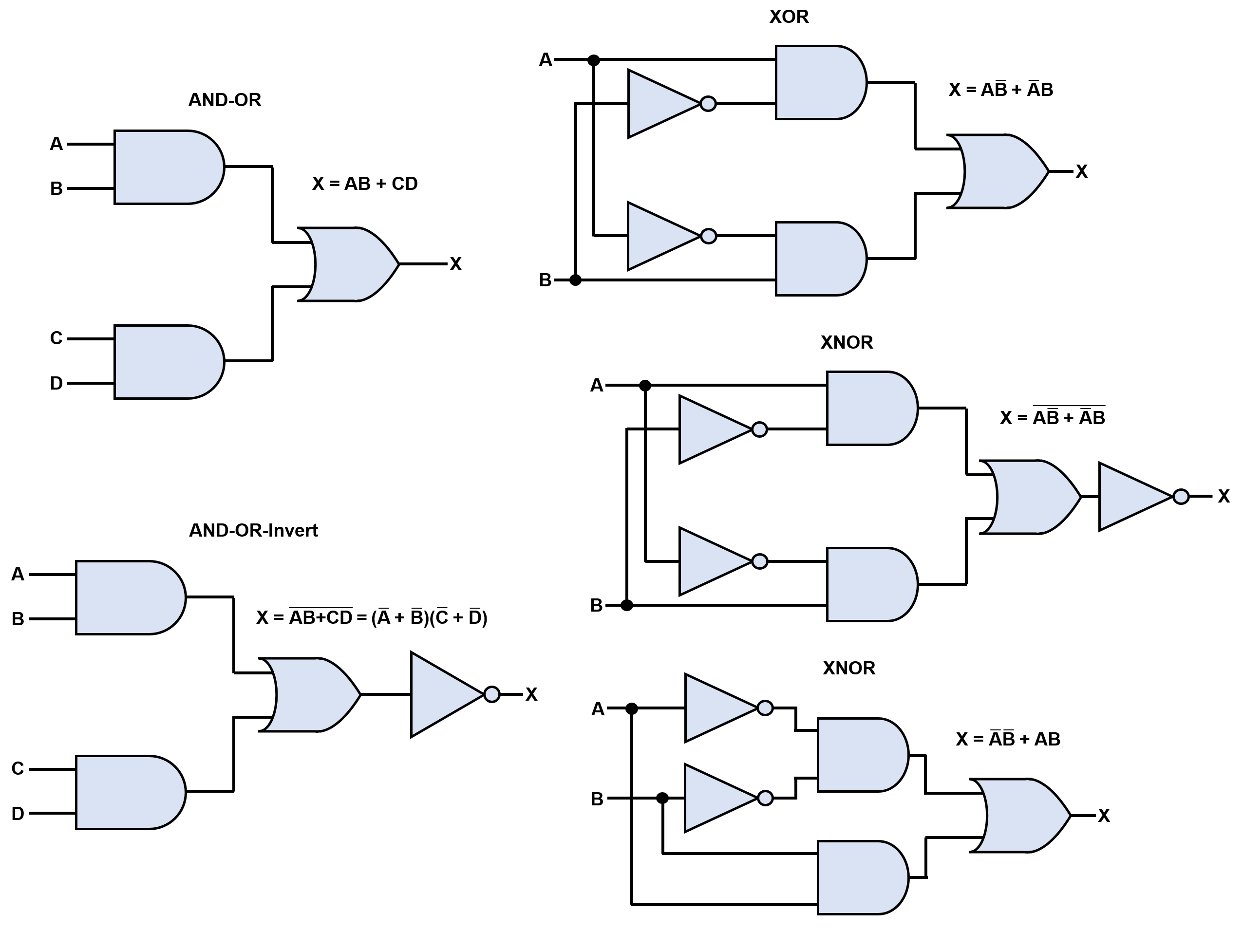
As described earlier, SOP expressions can be implemented via using AND logic gates as inputs to an OR logic gate output. This is called AND-OR logic. Another important type of logic is using AND logic gates as inputs to an OR logic gate and subsequently inverting the output of the OR gate. This is called AND-OR-Invert logic. To build a XOR gate (referred to as exclusive-OR logic), two AND gates, one OR gate, and two inverters are organized as shown in the figure below. To build a XNOR gate (referred to as exclusive-NOR logic), AND gates, OR gates, and inverters can be organized in multiple ways as shown in the figure below.
Implementing combinational logic from a Boolean expression requires recalling that Boolean multiplication is equivalent to an AND gate, Boolean addition is equivalent to an OR gate, and complementation is equivalent to a NOT gate (inverter). To implement combinational logic from a truth table, first convert the truth table to a Boolean expression via the method described in the truth table section. If a minimized Boolean expression is required, use a Karnaugh map as described in the section on Karnaugh maps.
Universal properties of NAND and NOR gates
The NAND gate is a universal gate because it can be used to make NOT, AND, OR, and NOR functions. The configurations of NAND gates needed to construct these functions are displayed below at left. The NOR gate is a universal gate because it can be used to make NOT, AND, OR, and NAND functions. The configurations of NOR gates needed to construct these functions are displayed below at right.

Combinational logic with NAND and NOR gates
NAND gates can be used to construct AND-OR logic systems (which implement SOP expressions). To do this, connect the output terminals of one or more NAND gates to the input terminals of another NAND gate. Note that the latter NAND gate is acting as a negative-OR gate.
Recall that, when a NAND gate is used to take one or more 0 inputs (i.e. 00, 01, 10 for a device with two inputs), it acts as a “negative-OR” gate. In this case, any of the 0 inputs will give an output of 1, so the operation is similar to OR. Any NAND gate carrying out a negative-OR operation is represented by the alternative symbol at right.
When drawing a combinational logic circuit with both NAND gates and negative-OR 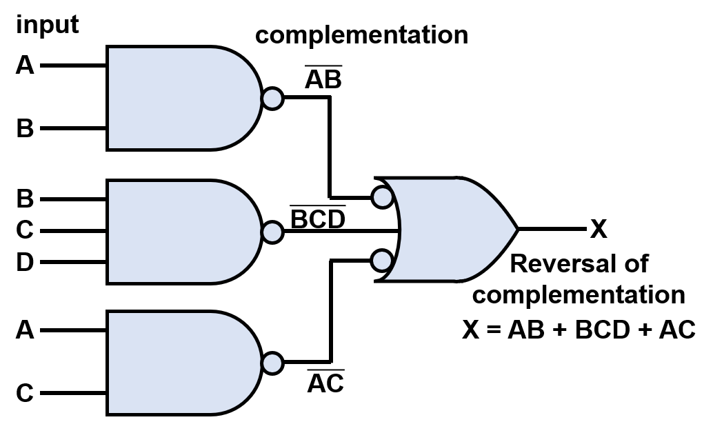 gates, the symbols should be drawn with NAND gate bubbles facing negative-OR gate bubbles to help make it easier to visualize how the inversion properties of the gates are cancelling each other out (a bubble represents that a gate carries out inversion as at least part of its operation).
NOR gates can be used to construct logic systems which implement POS expressions. To do this, connect the output terminals of one or more NOR gates to the input terminals of another NOR gate. Note that the latter NOR gate is acting as a negative-AND gate.
Recall that, when a NOR gate is used to take all 0 inputs (i.e. 00 for a device with two inputs), it acts as a “negative-AND” gate. In this case, all the 0 inputs together will give an output of 1, so the operation is similar to AND. Any NOR gate carrying out a negative-AND operation is represented by the alternative symbol at right.
When drawing a combinational logic circuit with both NOR gates and negative-AND gates, the symbols should be drawn with NOR gate bubbles facing negative-AND gate bubbles to help make it easier to visualize how the inversion properties of the gates are cancelling each other out. (As mentioned, a bubble represents that a gate carries out inversion as at least part of its operation).
Pulse waveform operation
The voltage or current signals associated with electronic circuits are often represented using trains of pulsed square waves. When a square wave is at its “HIGH” level of voltage or current, it represents a 1. When a square wave is at its “LOW” level of voltage or current, it represents a 0. Although these square waves are ideal forms of messier pulse trains, the binary qualities of digital electronic systems filter out the noise, allowing many analyses to be carried out with ideal square wave pulse trains.
In digital electronics, all waveforms are synchronized to a periodic waveform called the clock which keeps time for the system. All signals within the system are measured against the rate of periodic pulses from the clock. The clock sets the unit of time which denotes a single HIGH or LOW pulse state. This makes it so that the signals can pass through circuit elements (e.g. logic gates) at the appropriate time points and therefore perform appropriate operations.
Timing diagrams compare the signal trains within a digital system. Within each of these units of time, the waveforms for signal trains within the system might take on any combination of HIGH and LOW states.

In the context of logic gates, timing diagrams help to establish what inputs are arriving at which logic gates at what times. To review, the output of an AND gate at a given time is only HIGH if all of its inputs at the given time are HIGH, the output of an OR gate at a given time is only HIGH if at least one of its inputs at the given time are HIGH, the output of a NAND gate at a given time is LOW only when all of its inputs at the given time are HIGH, and the output of a NOR gate at a given time is LOW only when at least one of its inputs at the given time are HIGH.
Binary arithmetic
In digital systems, binary arithmetic serves as an essential mathematical language. It is especially vital for constructing complex combinational logic circuits which perform useful functions. As a starting point, the first fifteen binary numbers are 0, 1, 10, 11, 100, 101, 110, 111, 1000, 1001, 1010, 1011, 1100, 1101, 1110, 1111. These correspond to 1-15 in the base-10 system. Binary uses a base-2 system rather than a base-10 system. As will be explained in the following paragraphs, there are tricks which help to interconvert between binary and base-10 numbers.
The columns of a binary number can be thought of as representing the of base-10 values which sum up to the binary number’s base-10 equivalent where the nth column from right to left equals 2n starting with n = 0. To explain this, consider the following example. The binary value of 1011 is equal to eleven in the base-10 system. From right to left, 20•1 + 21•1 + 22•0 + 23•1 = eleven. This technique can be employed to convert any binary number to a base-10 number. Going the other way, one can convert a base-10 number to a binary number by finding the binary weights wi that cause the sum of 2n•wi to add up to the desired binary value.
To convert a base-10 decimal number to a binary fraction, a similar method is used, but negative binary weights are used for the part of the decimal number which is less than one. For instance, 2-1 = 0.5 and 2-2 = 0.25. In addition, a decimal point is inserted into the final binary number and the n within 2-n grows from left to right. As an example, consider that the base-10 decimal number 0.75 = 2-1•1 + 2-2•1, so its binary fractional equivalent is 0.11. Likewise, a binary fraction can be converted to a base-10 decimal number by finding the binary weights wi that cause the sum of 2n•wi + 2-n•wi to add up to the desired base-10 decimal number.
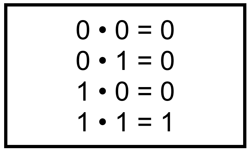
Binary addition is summarized in the box below. The top part describes the basic 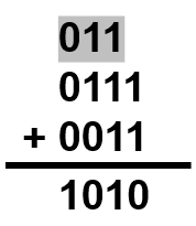 rules for addition of two bits (a bit is a single binary value) and the bottom part describes the rules for the addition of two bits plus a carry bit, which is a value that is carried in the same way as in base-10 addition. The carry bits are highlighted in gray. To illustrate this concept, an example of binary addition with carrying is also shown at right.

Binary subtraction is summarized in the box below. When performing binary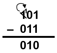 subtraction, a borrow is only needed if subtracting a 1 from a 0 digit (e.g. 110 – 1). To borrow, take a 1 from the column to the left, create a 10 in the column undergoing subtraction, and apply the rule 10 – 1 = 1. To illustrate this concept, an example of binary subtraction with borrowing is also shown at right.


Basic binary multiplication rules are summarized in the box below. To multiply two binary numbers, the top number is multiplied by each digit of the bottom number from right to left. The first of these partial products is not shifted left, the second is shifted left by place, the third is shifted left by two places and so on. After shifting, 0 values are put in the empty slots. The partial products are then summed to obtain the result. To illustrate this concept, an example of binary multiplication with shifting is shown at right.
To perform binary division, one must (1) set up long division. The quotient goes on the top, the dividend goes under the quotient, and the divisor goes to the side of the dividend. (2) Place a copy of the divisor below the dividend but align it to the leftmost digits of the dividend. (3) If the part of the dividend above the divisor is greater than or equal to the divisor, then subtract the divisor from that part of the dividend, place the 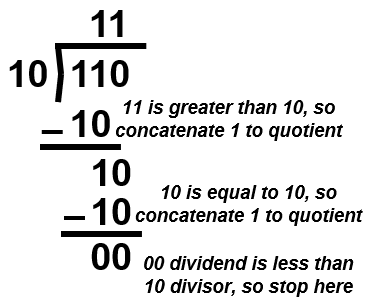 result of the subtraction below, and concatenate a 1 to the rightmost end of the quotient. If the dividend above the divisor is less than the divisor, concatenate a 0 to the rightmost end of the quotient. (4) Place another copy of the divisor at the bottom but shift it one column to the right. (5) Repeat steps 3 and 4 until the part of the dividend is less than the divisor. The result is the quotient with the dividend as a remainder. To illustrate this concept, an example of binary division is shown at right.
Half-adders and full-adders
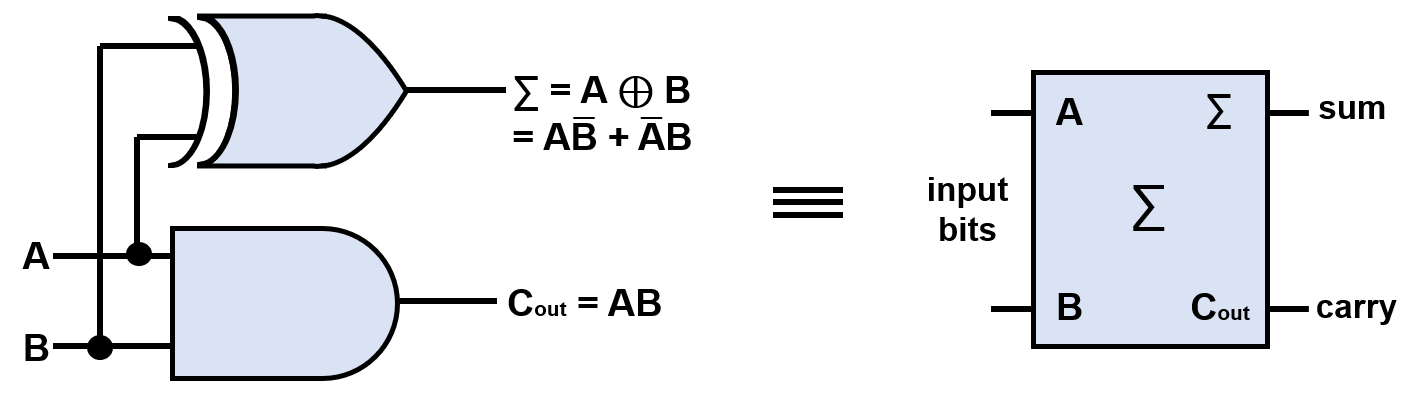
Half-adders take in two input bits and subsequently generate a sum bit and a carry bit, performing the first step in binary addition. Half-adders implement the basic rules of binary addition: 0 + 0 = 0, 0 + 1 = 1, 1 + 0 = 1, and 1 + 1 = 10. Because XOR gates only produce outputs of 1 when the inputs are not equal, a XOR gate is used to generate the sum bit. Because AND gates only produce outputs of 1 when the inputs are both 1, an AND gate is used to generate the carry bit. The truth table for a half-adder is displayed at right. The logic gate diagram for a half-adder is shown below at left and the equivalent logic symbol is shown below at right.
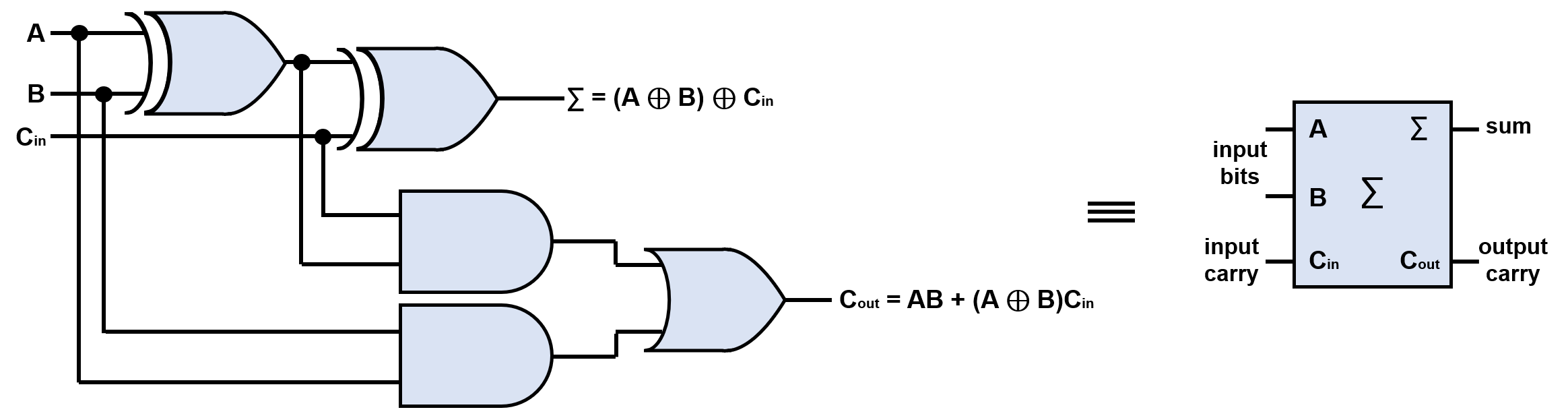
Full-adders take in two input bits and an input carry and subsequently generate a sum bit and an output carry before performing the OR operation on them. In other words, full-adders can implement the addition of two 1-bit numbers and an input carry. To see how this corresponds to the rules for binary addition, refer to the box in the 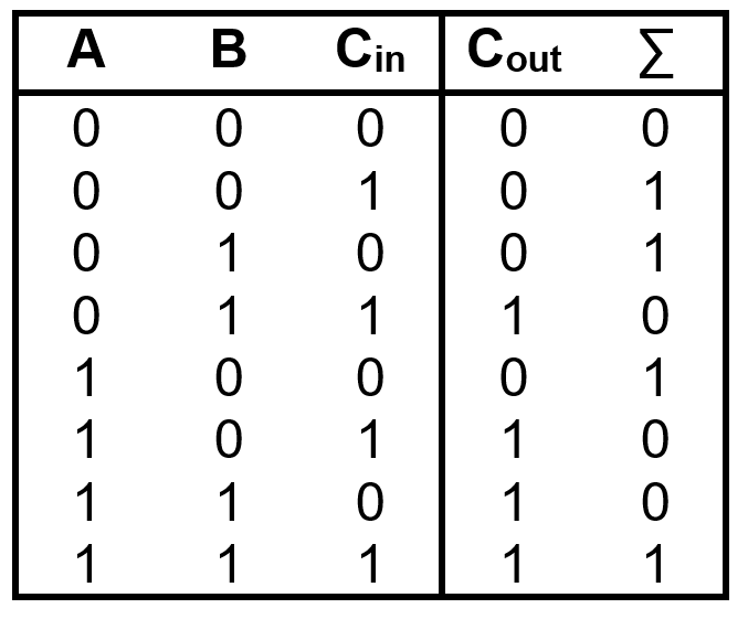 section on binary addition. Since the sum of the two input bits is A⊕B, the sum of the two input bits and the input carry is (A⊕B)⊕Cin. (Note that the circled plus indicates the XOR operation). The equation for the output carry is Cout = AB + (A⊕B)Cin. Full-adders are composed of two half-adders and an OR gate. The truth table for a full-adder is displayed at right. The logic gate diagram for a full-adder is shown below at left and the equivalent logic symbol is shown below at right.
Parallel binary adders
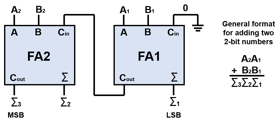
Parallel binary adders are composed of two or more full adders and are used to add binary numbers of more than one bit. To add two binary numbers, a full-adder is needed for each bit in the numbers (e.g. for a 2-bit number, two full-adders are necessary). The least significant bit of the output is often grounded to make it zero since there is no carry input to the least significant bit (LSB) position. Note that there is also a most significant bit position (MSB) at the other end of the system. The block diagram for a 2-bit parallel adder alongside the addition operation it performs are shown below.
Extension of these concepts to 4-bit parallel adders and beyond is straightforward. The output carry terminal of each full-adder is linked to the input carry of the next full-adder in the lineup (these links are known as internal carries). In this way, larger binary numbers can undergo the sum operation. As an example, the block diagram for a 4-bit parallel adder and its equivalent logic symbol are shown below.

The truth table for a the 4-bit adder example is shown at right. The subscript n represents the adder bits. Cn – 1 represents the carry from the previous adder. Carries 1, 2, and 3 are internal carries while carry 4 is an output carry and carry 0 is an input carry.
Ripple carry adders are a category of parallel binary adder which have the output carry of each full-adder connected to the input carry of the next full-adder in the sequence. The sum and the output carry of any stage (a single full-adder is one stage) cannot be produced until the input carry occurs, causing time delays associated with each successive stage. The input carry to the LSB stage must move through all of the stages before a final sum is obtained. Because of this, the cumulative delay is assumed as the number of stages multiplied by the maximum amount of time for the signal to pass through each stage. For an individual ripple carry adder, this cumulative delay is often on the order of tens of nanoseconds.
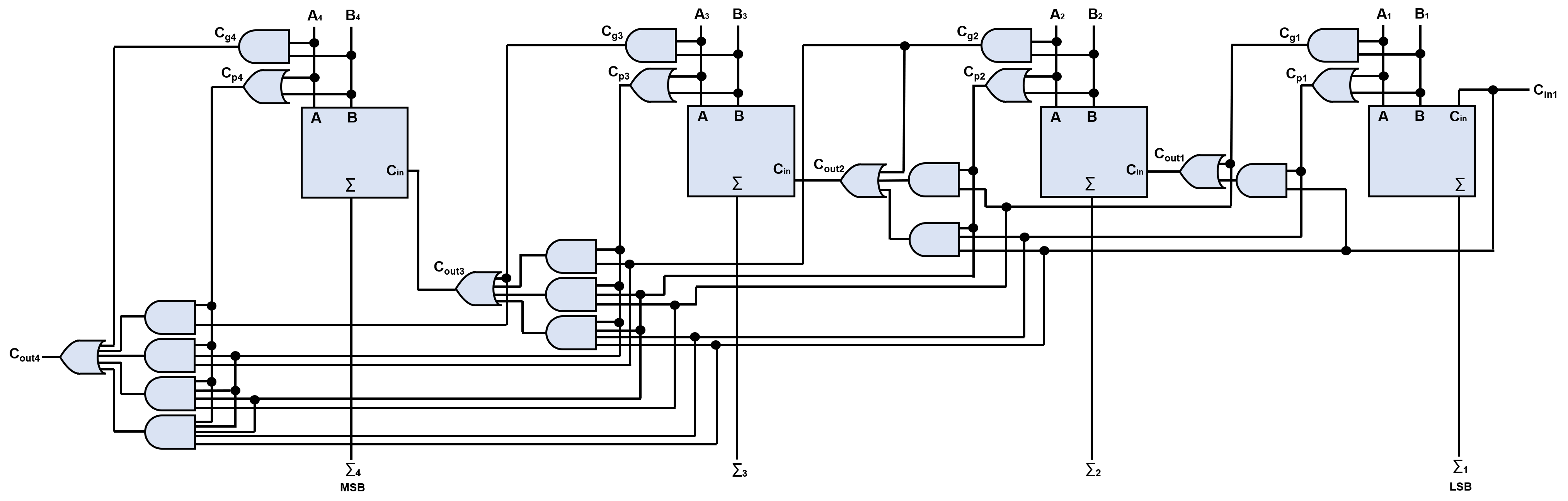
Look-ahead carry adders are a category of parallel binary adder which eliminate the ripple carry delay and so operate more efficiently than ripple carry adders. To eliminate the ripple carry delay, look-ahead carry adders generate a carry only when both of the input bits are 1s. The input carry then propagates within its full-adder to the output carry. The generated carries are denoted Cg and the propagated carries are denoted Cp. The output carry of a single full-adder can be expressed in Boolean algebraic terms as Cout = Cg + CpCin. In parallel binary adders, the Cin of each successive stage equals the Cout of the previous stage. Since each Cg and Cp is expressible in terms of the A and B input bits (to the full-adders), all of the output carries are available almost immediately and it is not necessary to wait for the carries to ripple through all of the stages. The logic gate implementation of a 4-bit look-ahead carry adder is displayed below.
Comparators
Comparators compare two binary numbers and determine relationships between those quantities. The simplest type of comparator decides if two binary numbers are equal. An XNOR gate can act as a comparator to decide if the input bits are equal, giving an output of 1 if the inputs are equal and giving an output of 0 if the inputs are unequal. To expand this to numbers consisting of more bits, the output terminals of multiple XNOR gates are linked to the input terminals of an AND gate. In this way, all of the bits comprising the two numbers must be equal in order for the two numbers themselves to be equal. As an example, a 4-bit comparator and is shown below.

There are also magnitude comparators which can determine whether a binary number is greater than or less than another binary number. To do this, the magnitude comparator must examine if the MSB of number A is greater than, less than, or equal to the MSB of number B. If AMSB > BMSB, then A > B, if AMSB < BMSB, then A < B, and if AMSB = BMSB, then the same process must be performed upon the next most significant bit in the number. The steps are repeated until the relationship between the two numbers is determined. The output which correctly describes the relationship between the two numbers is 1 and the other two outputs are 0. As an example, a logic gate implementation of a 2-bit magnitude comparator and its equivalent logic symbol are shown below.

Decoders
Decoders give an output of 1 when a certain binary number is used as an input and they give an output of 0 for any other binary number input. For example, a decoder might detect the binary number 1001 and output 1 only when the inputs are 1001.
To perform their function, decoders must convert all the 0s of the targeted number 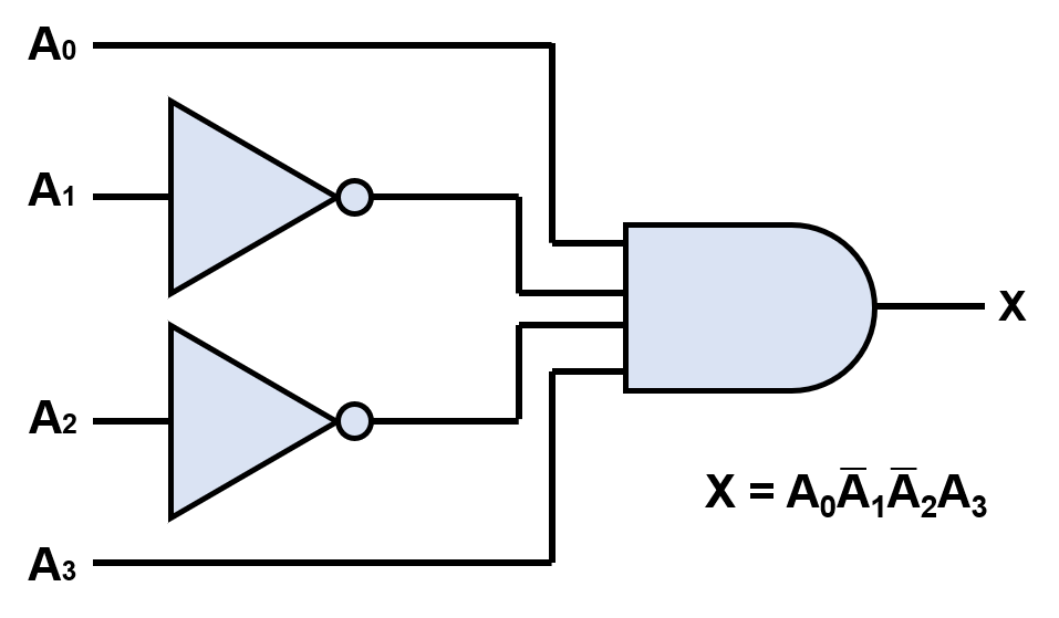 into 1s via NOT gates and then feed every input to an AND gate. Since the AND gate will only output 1 when all inputs are 1, the targeted number will be detected through the NOT gates converting all 0s in the targeted number to 1s. As an example, the logic gate implementation of a decoder which detects 1001 is shown at right.
One can also construct a decoder using a NAND gate in place of the AND gate. In the NAND gate version, an output of 0 indicates that the specified binary number has been detected.
One common type of decoder configuration is a decoder which takes in n bits and decodes every one of the 2n possible combinations of those bits. These decoders typically operate by the same principle as described above, though they must send their n inputs to 2n AND gates or NAND gates (depending on whether the active output needs to be a 1 or a 0). For example, a 4-line-to-16-line decoder receives a 4-bit input and outputs a 1 from a different terminal when it detects each of the 16 distinct combinations of 4 bits. To illustrate this, the truth table of a 4-line-to-16-line decoder which uses AND gates is displayed below.

Because this type of decoder outputs a 1 (or a 0 if NAND gates are used) corresponding to each of the possible 4-bit binary inputs, it can be used to convert 4-bit binary numbers to base-10 numbers. For instance, the binary value 1110 is equivalent to the base-10 value of 14 and 1110 activates the 14th output terminal. The logic symbol for a 4-line-to-16-line decoder (with 1s as active outputs) is displayed below.

There are other similar decoders that act as standard parts for binary to base-10 conversion. In particular, the BCD-to-decimal converter (“decimal” is another name for base-10 numbers and “BCD” stands for Binary Coded Decimal) or 4-line-10-line decoder uses the same setup as the 4-line-to-16-line decoder, but it only has ten outputs. These ten outputs correspond to the base-10 values of zero through nine. Once again, the active output is 1 if AND gates are used and is 0 if NAND gates are used. Another common decoder is the BCD-to-7-segment decoder, which has a 4-bit input and gives one of seven outputs depending on the input. This decoder also operates on the same principle as the 4-line-to-16-line decoder. However, the BCD-7-segment decoder is used to control the images formed on a seven-segment display device such as a handheld calculator.
Encoders
An encoder first receives an active input on one of its input terminals. The input often represents a digit (such as a base-10 digit), an alphabetic character, or another symbol. Next, the encoder translates this input into a coded output such as a binary value.
One common type of encoder is the decimal-to-BCD encoder. As alluded to in the previous section, BCD code is a way of representing base-10 numbers using 4-bit binary values. The BCD code uses the first ten binary numbers (0000 to 1010) to represent base-10 values of 0 to 9.
The decimal-to-BCD encoder has inputs of 0, 1, 2, 3, 4, 5, 6, 7, 8, and 9 and outputs of A3, A2, A1, and A0. Decimal-to-BCD encoders use OR gates to convert each input to its appropriate output. The logic of this (assuming 1 as the active value) is as follows. Bit A3 only outputs a 1 for base-10 digits 8 or 9, bit A2 only outputs a 1 for base-10 digits 4 or 5 or 6 or 7, bit A1 only outputs a 1 for base-10 digits 2 or 3 or 6 or 7, and bit A0 only outputs a 1 for digits 1 or 3 or 5 or 7 or 9. To better understand this, it is helpful to examine the decimal-to-BCD truth table above. The logic gate implementation for a decimal-to-BCD encoder is displayed below alongside its corresponding logic symbol. Note that an input for the base-10 zero digit is not needed since, when all of the binary inputs are 0, the binary outputs are 0000.

Another similar type of encoder is the decimal-to-BCD priority encoder. This type of encoder is configured to include a priority function. As a result, if multiple inputs are given to the decimal-to-BCD priority encoder, the binary output will represent only the largest base-10 value that was used as an input. By comparison, the decimal-to-BCD encoder without the priority function must have only one active input to work properly.
Code converters
It is often necessary in electronic systems to convert between different digital codes. Though there are others, one important type of code converter is the BCD-to-binary converter. This type of code converter can help to illustrate the general idea of code conversion in digital electronics.
From a mathematical standpoint, to perform BCD-to-binary conversion, one must first weight the BCD digits depending on their position within the BCD number. For instance, a decimal value of 27 is represented in BCD as 00100111. In BCD code, the 0010 corresponds to the 2 in the tens place and the 0111 corresponds to the 7 in the ones place. The weights of the tens place are 80, 40, 20, 10 and the weights of the ones place are 8, 4, 2, 1.
In BCD-to-binary circuits, the binary representations of the weights of the BCD bits are added to obtain the corresponding binary number. For the case of 00100111, this is 1•20 + 1•4 + 1•2 + 1•1 = 27 in decimal form and 1•10100 + 1•100 + 1•10 + 1•1 in binary form (the parts that are multiplied by 0 have been excluded here since they equal 0). The BCD-to-binary conversion can be implemented using adder circuits to sum the weighted binary numbers.
Multiplexers
Multiplexers (or data selectors) are devices which take in data from multiple sources and route those data into a single transmission line to send them to a common destination. The way that a multiplexer works is that it receives both data-select lines and data-input lines. Bits sent to the data-select lines control which of the data-input lines is transmitted to the single data-output line.
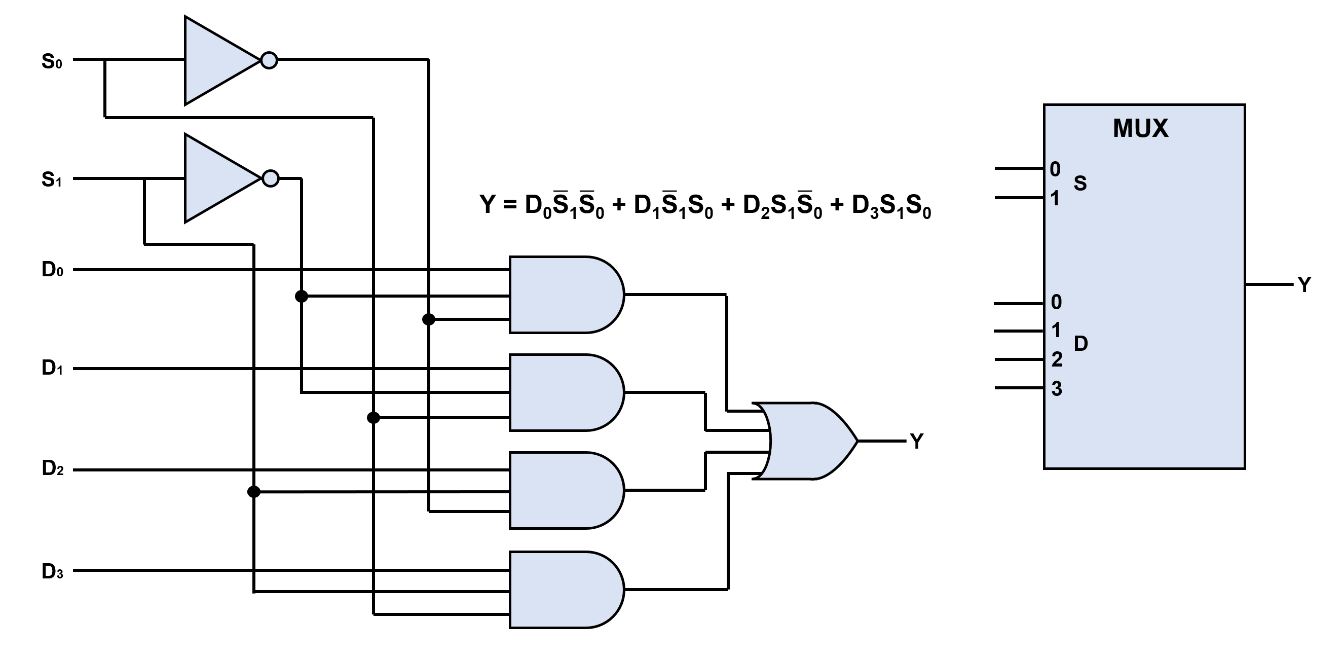
As an example, consider a 4-bit multiplexer. The 4-bit multiplexer receives two data-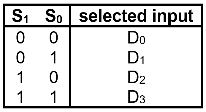 select lines which control four data-input lines. The four possible inputs to the data-select lines (00, 01, 10, and 11) control which of the four data-input lines undergoes transmission to the data-output line. The truth table for this device is displayed at right where S1 and S0 are the data-select lines.
To understand how to implement a 4-bit multiplexer using logic gates, it is helpful to see that the Boolean expression below describes the multiplexer’s operation. Y represents the data output. Recall that OR gates implement Boolean addition, AND gates implement Boolean multiplication, and NOT gates implement Boolean complementation. The logic gate implementation and corresponding logic symbol of a 4-bit multiplexer are given along with the Boolean expression.
The principles of 4-bit multiplexers can readily be extended to any n-bit multiplexers. For a given n-bit multiplexer with n data-input lines, log2(n) data-select lines would be necessary. The logic gate implementation would depend on a Boolean expression analogous to the one above, but with more input variables and more of their corresponding data-select bit combinations.
Demultiplexers
Demultiplexers take information from a single input line and send the information to a given number of output lines. As with multiplexers, demultiplexers also take data-select inputs to determine to which output line the data are sent.
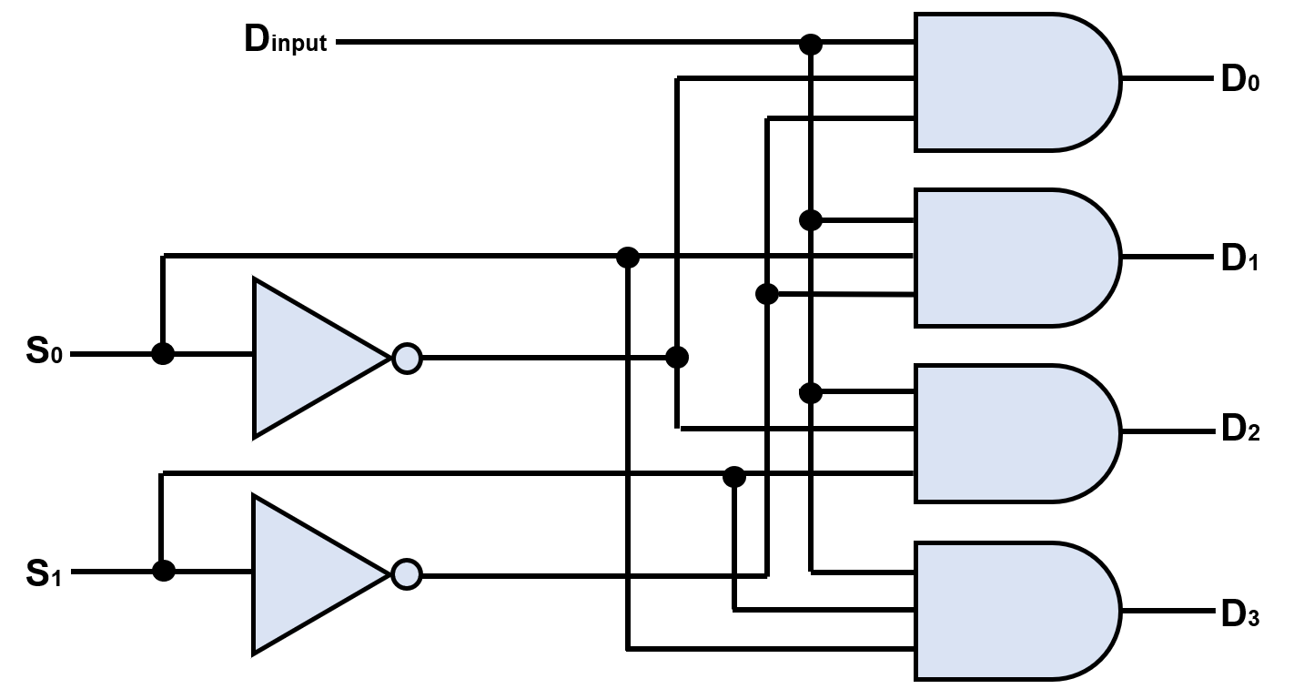
To illustrate how demultiplexers work, consider a 1-line-to-4-line demultiplexer. The logic gate implementation for a 1-line-to-4-line demultiplexer is displayed below. This demultiplexer receives a single data-input line which goes to all of the AND gates. It also receives two data-select lines which control which of the AND gates transmits the data-input line. Since all inputs to an AND gate must be 1 in order for the AND gate to transmit a 1, the data-select lines make it possible to choose which AND gate receives all 1 inputs. Using the data-select lines, only one of the data-output lines will transmit the information at a time.
The principles of demultiplexers in general can readily be found by extending the concept of the above demultiplexer. For a demultiplexer with n data-output lines, log2(n) data-select lines are needed to control where the data-input line signal is sent.
Modified decoders are also usable as demultiplexers. When a decoder is used as a demultiplexer, its input lines are used as data-select lines since they determine which of the output lines sends an active signal. The modification needed is an enable gate. If the enable gate is not active on both inputs, the decoder cannot transmit any active outputs. By fixing one of the enable gate’s inputs as permanently active, the other input to the enable gate can behave as the data-input line. In this way, the decoder acts as a demultiplexer.
Parity checkers
Parity is a method of error detection. For a given system, any set of bits contains either an even or an odd number of 1s. Depending on the system, the parity bit is attached to a set of bits to make it so that the total number of 1s in the given system is always even or so that the total number of 1s in the given system is always odd. If a system operates with even parity, a parity check is made on each set of bits to make sure that the total number of 1s is even. If a system operates with odd parity, a parity check is made on each set of bits to make sure that the total number of 1s is odd. In the case that these conditions are not met, the system in question reports an error.
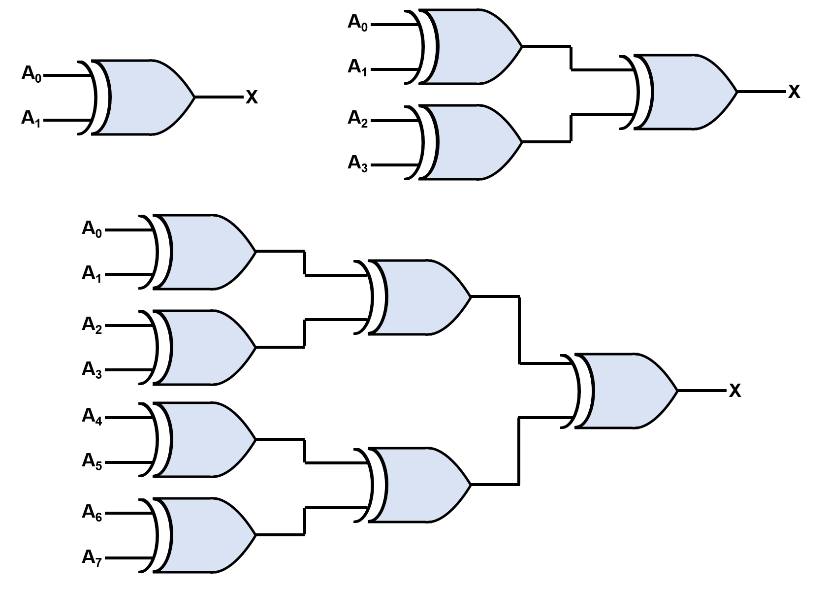
To determine if a code has even parity or odd parity, all of the bits in that code are added together. Two bits can be summed using a single XOR gate, four bits can be summed using a pair of XOR gates with their output terminals linked to the input terminals of a third XOR gate, and so on. It is important to note that the sum is a modulo-2 sum. This is a binary sum where a 0 results whenever a carry would otherwise occur (0 + 0 = 0, 0 + 1 = 1, 1 + 0 = 1, 1 + 1 = 0). If a set of bits contains an even number of bits, the XOR gate system will produce a 1. If a set of bits contains an odd number of bits, the XOR gate system will produce a 0. The XOR gate implementations of parity checkers for sets of two, four, and eight bits are given below.
Reference: Floyd, T. (2015). Digital Fundamentals, Global Edition. Pearson Education Limited.
Cover image source: SciTechDaily.com
